Materials Testing and Investigation Services
The Rimkus Materials Testing and Investigation team specializes in material failure analysis, corrosion investigation, and weld engineering. We also offer a wide variety of professional materials testing, analysis, and consulting services.
By performing a comprehensive failure analysis, the root causes of material failures can be identified, metallurgical problems may be solved, and recommendations can be made to prevent future recurrence. Using advanced analytical equipment and techniques, our materials experts can interpret test results and provide clients with a detailed plan of action.
The professional staff also specialize in many other areas of materials engineering including, but not limited to, defect investigation, heat treatment processes, reverse engineering, coatings and platings, vendor qualification, and material selection.
Businesses and industries from around the world rely on the professional staff at Rimkus Materials Testing and Investigation to provide them with fast and accurate materials testing results. Some of these industries include Motorsports, Automotive Manufacturing, Plumbing (Water Systems), Marine, Chemical and Pharmaceutical Production, Power Generation and Utilities, Heat Exchangers, and Boilers.
Learn more about our Materials Testing and Investigation laboratory services below or by contacting us directly at (704) 663-5108 or materialslab@rimkus.com.
Rimkus also has a dedicated team of experienced consultants for materials matters involving insurance and litigation. Visit our Materials Science and Engineering page to learn more.

James F. Lane, P.E.
Director, Materials Science Practice and Laboratory Services
(312) 639-9321 jflane@rimkus.com
Our Materials Testing and Investigation Services
-
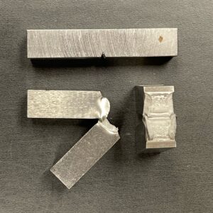
Failure Analysis
 Failure analysis is performed by systematically examining, testing, and analyzing components to identify the cause and sequence of events that lead to a product failure. This specialized testing can vary significantly depending on the result found. This process typically involves the following steps:
- Gathering information about the component, its application, and its history
- Detailed visual examination
- Photo documentation of the components and visual evidence
- Non-destructive testing
- Low-magnification stereoscope examination or 3D imaging
- High-magnification scanning electron microscopy (SEM) examination
- Elemental analysis spectrometry/SEM
- Sectioning the sample for metallographic microanalysis
- Metallography
- Hardness testing
- Chemical analysis
- Mechanical testing
- Detailed evidence and data review
- Formulation of a professional conclusion and opinion
- Interoperative report of our findings and recommendations
-
Corrosion Investigation
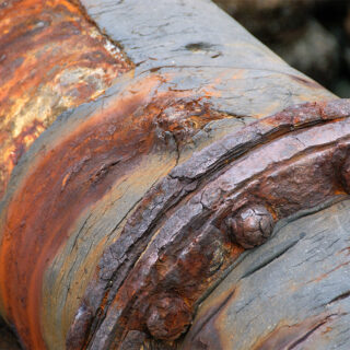 Corrosion is a chemical reaction phenomenon that results in degradation of material and can lead to serious or catastrophic failures. Corrosion investigation engineering is the process of collecting corrosion failure samples and analyzing them to determine the source (root cause) and severity of the corrosion. Drawing from these analyses, we provide expert opinions and recommendations for corrosion remediation and prevention. The Rimkus Materials Testing and Investigation team specializes in corrosion investigation engineering and the analytical techniques used to identify corrosion mechanisms. We have the expertise to recommend more corrosion-resistant alloys or coatings for a particular application or environment to prevent recurrent corrosion issues. Our energy dispersive X-ray spectroscopy (EDS) system can analyze corrosion deposits to identify the corrosive agent. We also have the expertise and capabilities to offer accelerated salt fog and other corrosion testing to determine the suitability of materials and coatings for specific environments.
 -
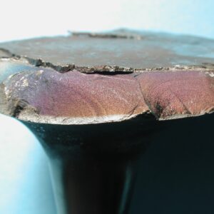
Weld Engineering
 A significant amount of metallurgical engineering is needed to successfully produce sound weldments in mechanical and structural applications. We can provide welder and welding procedure qualification testing to ensure compliance with a wide variety of industrial specifications such as those set by the American Welding Society (AWS) and the American Society of Mechanical Engineers (ASME). We perform weld testing to evaluate the soundness, toughness, brittleness, hardness, and other properties of weldments before production begins. Our team also frequently investigates weld failures to determine the root cause of fracture or degradation of the weldment in the field. Welder and Welding Procedure Qualifications:
- Bend Testing
- Charpy Impact (CVN) Testing
- Florescent Dye Penetrant
- Visual Inspection
- Macro-Etch Testing
- Tensile Strength
-
Scanning Electron Microscopy
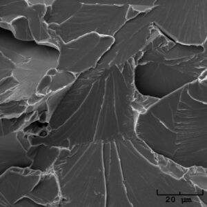 Our scanning electron microscope (SEM), with the addition of the energy dispersive X-ray spectrometer (EDS), can examine and analyze samples at magnifications typically ranging from 5X to 20,000X. Using our state-of-the-art scanning electron microscope, our experts can analyze everything from microstructure and fracture surface to corrosion products, pitting, and impurities within the material. The fracture surface topography revealed at increased magnification can reveal an exorbitant amount of information:
- Type of stress (tensile, shear, torsional)
- Mode of fracture (ductile, brittle, fatigue, overload)
- Direction of fracture propagation
- Area and mechanism of fracture initiation
- Contamination within the microstructure
- Elemental analysis of corrosion products and deposits
- Elemental composition of very small parts
- Manufacturing- or repair-related factors contributing to the failure
- Other factors related to the cause of the failure
-
Energy Dispersive Spectroscopy
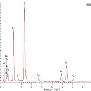 Using a scanning electron microscope (SEM) with an energy dispersive X-ray spectrometer (EDS) is an advanced analytical technique that enables the operator to identify the chemical characterization/elemental analysis of materials. EDS analysis can identify the elemental composition of fine to microscopic particles or larger regions on the surface of samples. During an SEM examination, the locations, deposits, or areas of interest are analyzed using an EDS attached to the scanning electron microscope. EDS microanalysis is performed by measuring the energy and intensity of the signals generated by a focused electron beam scanned across the specimen. Elemental Dot Map Element mapping measures the individual elemental distributions on the exposed surface of a sample. Typically, this technique produces an analysis of one field of view by utilizing the scanning electron beam in conjunction with the EDS detector, in a grid pattern to produce a map. This analysis is particularly valuable when identifying contamination, coating/plating layers, diffusion during welding, and corrosion products.
 -
Non-Destructive Testing
 Rimkus Materials Testing and Investigation experts utilize a variety of non-destructive testing techniques, including:
- Energy dispersive spectroscopy (EDS)
- Scanning electron microscopy (SEM)
- High-resolution 3D surface profile
- 3D profile measurements
- Surface finish/roughness
- Liquid Penetrant Testing (PT)
- Various types of liquid PT methods are utilized to detect material defects open to the surface or to detect open surface cracks. Red dye or fluorescent penetrants are utilized as well as various types of wet and dry developers.
- Magnetic Particle Inspection (MPI)
- Process for detecting surface and shallow subsurface discontinuities in ferromagnetic materials
- Portable Hardness
- Rockwell, Brinell, Leab
- Visual and Low Magnification Inspection
- Portable X-ray Fluorescence (XRF) Spectrometer
- Energy dispersive spectroscopy (EDS)
-
Metallography (Microstructure Evaluation)
 Metallography is the study of the microstructures of metallic materials. The properties of a material and its performance in a specific application depend on its microstructure. Rimkus utilizes numerous types and magnification of high-resolution optical and digital microscopes during the metallurgical examination process. Analyses of microstructure in cross-sectioned samples help determine material properties, fracture propagation, corrosion pitting morphology, heat treatment, quality and thickness of plating and coating, grain size, overheat damage, material contamination, flaw characteristics, weld quality, manufacturing design flaws, and defect mechanisms. The Rimkus Materials Testing and Investigation team has advanced training and knowledge in metallographic preparation procedures/processes, from sectioning and mounting the specimen through the grinding and polishing stages to proper selection and etching techniques of the tested material. Our expert laboratory staff is looked upon to provide metallurgical samples preparation techniques and their subsequent interpretations to clients from across the country.
 -
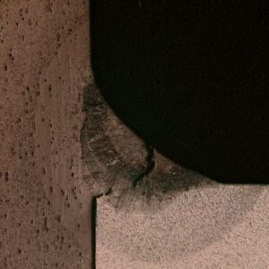
Defect Investigation
 During manufacturing, defects can be introduced at several stages of processing. Supported by the necessary advanced analytical equipment, expert training, and experience, the Rimkus Materials Testing and Investigation experts perform high level defect investigation to identify the specific processing step in which a defect occurred. Our experts will not only interpret the results but can provide recommendations to prevent future defects. By providing high-quality defect investigation along with other materials testing methods, our team can determine whether a product failed due to defects or flaws produced in the manufacturing process or if the failure was caused during normal or abnormal usage.
 -
Mechanical Testing
 Rimkus experts have extensive mechanical testing experience to determine the compliance of materials to applicable standards and specifications. We have significant knowledge of mechanical testing methodology and are highly skilled in interpreting the results. Our team can perform mechanical testing and materials testing as part of a quality assurance program, manufacturing engineering program, failure analysis, or for materials research and development. Tests can be performed to ASTM specifications or other industry-recognized standards. In-house mechanical testing equipment is used for the following materials tests:
- Bend Testing
- Tensile Testing
- Compression Testing
- CVN (Charpy V-notch) Testing
- Microhardness Testing (Knoop, Vickers)
- Rockwell Hardness
- Brinell Hardness
-
Reverse Engineering
 Reverse engineering is the method of identifying and analyzing the materials and processing used to manufacture components in order to create products with identical properties. By determining material properties such as chemical composition, heat treatment, coating type, and coating thickness, reverse engineering can be accomplished.
- Chemical Analysis
- Identifying the materials’ chemical composition
- Metallography/Microstructure Evaluation
- Cast
- Forged
- Extruded
- Surface treatments (nitride, carburized, etc.)
- Heat Treatment
- Hardness or microhardness traverse
- Effective case depth
- Microstructure
- Coatings
- Plating
- Cladding
- Anodized, phosphate, conversion coatings, etc.
- Chemical Analysis
-
Chemical Composition Analysis
 An invaluable component of a failure analysis or corrosion investigation is the chemical analysis of metals. Used for multiple purposes, chemical analysis is crucial in the identification of manufacturing difficulties, completion of quality control requirements, and reverse engineering of components that need to be recreated. Material chemical composition analysis and verification ensures that each component or raw stock material is produced in accordance with the correct material alloy specification. Chemical composition analysis can be performed using various methods that compare results against the appropriate industry standards, such as ASTM, SAE, and more. Our team of experts routinely analyzes the alloying content of a wide range of materials including, but not limited to iron, steel, aluminum, copper, nickel, zinc, titanium, and lead. For metals, the Optical Emission Spectrometry (OES) technique utilizes a high-energy spark created between an electrode and a sample of the material to be analyzed. The spark creates an emission of radiation from the excited sample surface with wavelengths characteristic of the elemental chemical composition. The spectrum of radiation is separated into the distinct element lines and the intensity of each line is measured. Finally, these are precisely converted into concentration values for each element present. OES continues to be the reference technique for direct chemical analysis of solid metallic samples. The unmatched combination of accuracy, high speed, precision, stability, and reliability have made it an indispensable tool for production and verification of quality metal products.
 -
Field Microstructure Replication
 Field metallographic replication is a (semi) non-destructive test required in some applications where it is not possible to remove a component from service or the size of the components prohibits analysis in the laboratory. Assorted replicating media techniques allow our experts to create a portable copy of the microstructure of interest while in the field. Replication involves removal of the material’s surface by lightly grinding, followed by polishing using fine grits. Once the surface is properly polished and prepared, it is then etched with various acids to reveal the materials microstructure. The replicating media is then applied and allowed to cure. Once the replicating media is cured, it will be removed from the sample, returned to our laboratory, and analyzed using a variety of microscopes. Replication can also be performed to replicate surfaces for surface finish or other testing, replicating shapes, corrosion pitting, cracking or any other surface that require imaging or measurements.
 -
High-Resolution 3D Optical Surface Profiler
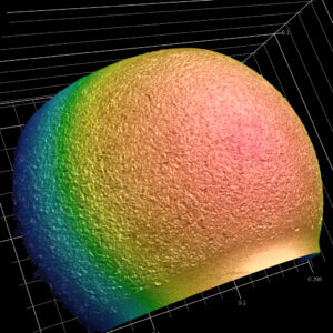 With its 6 x 11-inch fully automated stage, the high-resolution Keyence VR enhances our capabilities for measuring and analyzing large samples. It can be utilized in nearly all industries and at every step of engineering, from research and development to production, and from quality control through analysis of failures and defect investigation. The Keyence VR is just one of the many pieces of advanced technological and analytical equipment we utilize to assist customers in understanding their complex matters.
- Measurement of Complex Profiles
- The Keyence VR can scan any 2D or 3D object or surface and provide any type of 2D and 3D surface or profile measurement. It also allows for no-contact surface finish and roughness measurements and the evaluation of true surface flatness.
- Surface Finish and Roughness
- Surface finish and roughness testing can be completed in our lab, or in-situ onsite, with the use of our high-resolution, zero-shrinkage replication media.
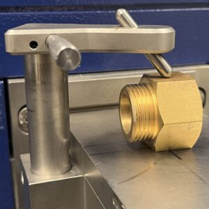
- Product Defect and Fit Up
- Was a rubber gasket installed improperly or was it defective from the manufacturer? Did the gasket seat match the gasket dimensions? We can use the high-resolution 3D profile measurements obtained by the Keyence VR to answer these questions.
- Manufacturing Defects
- We can use the Keyence VR for the evaluation of components (such as plumbing fittings) for any unusual wear scars, molding lines, deformities, thread damage, or corrosion pitting.
- Environmental Roofing Damage
- Environmental hail damage to shingles can be difficult to characterize and evaluate. With the use of the Keyence VR, we can evaluate, characterize, and confirm damage to roofing shingles.
- Non-destructive Analysis
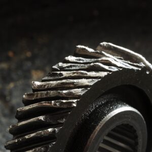
- 3D profile measurements of gears and bushings are now possible without destructive testing. This allows our project managers to evaluate wear patterns quickly and efficiently with high accuracy and repeatability.
- Injection Mold Defects
- Injection molds and dies can improperly wear, causing defects to the final product. We can now measure these wear scars and flaws to characterize and identify the dimensions of the molds and dies.
- Measurement of Complex Profiles
Our Materials Testing and Investigation Experts

Laboratory Operations Manager
Director, Materials Science Practice and Laboratory Services